- 您现在的位置:买卖IC网 > Sheet目录342 > MCBSTM32EXL (Keil)BOARD EVALUATION FOR STM32F103ZE
�� �
�
�Analog-to-digital� converter� (ADC)�
�RM0008�
�11.9.1�
�Note:�
�Injected� simultaneous� mode�
�This� mode� converts� an� injected� channel� group.� The� source� of� external� trigger� comes� from�
�the� injected� group� mux� of� ADC1� (selected� by� the� JEXTSEL[2:0]� bits� in� the� ADC1_CR2�
�register).� A� simultaneous� trigger� is� provided� to� ADC2.�
�Do� not� convert� the� same� channel� on� the� two� ADCs� (no� overlapping� sampling� times� for� the�
�two� ADCs� when� converting� the� same� channel).�
�At� the� end� of� conversion� event� on� ADC1� or� ADC2:�
�●�
�●�
�The� converted� data� is� stored� in� the� ADC_JDRx� registers� of� each� ADC� interface.�
�An� JEOC� interrupt� is� generated� (if� enabled� on� one� of� the� two� ADC� interfaces)� when� the�
�ADC1/ADC2� injected� channels� are� all� converted.�
�Note:�
�In� simultaneous� mode,� one� must� convert� sequences� with� the� same� length� or� ensure� that� the�
�interval� between� triggers� is� longer� than� the� longest� of� the� 2� sequences.� Otherwise,� the� ADC�
�with� the� shortest� sequence� may� restart� while� the� ADC� with� the� longest� sequence� is�
�completing� the� previous� conversions.�
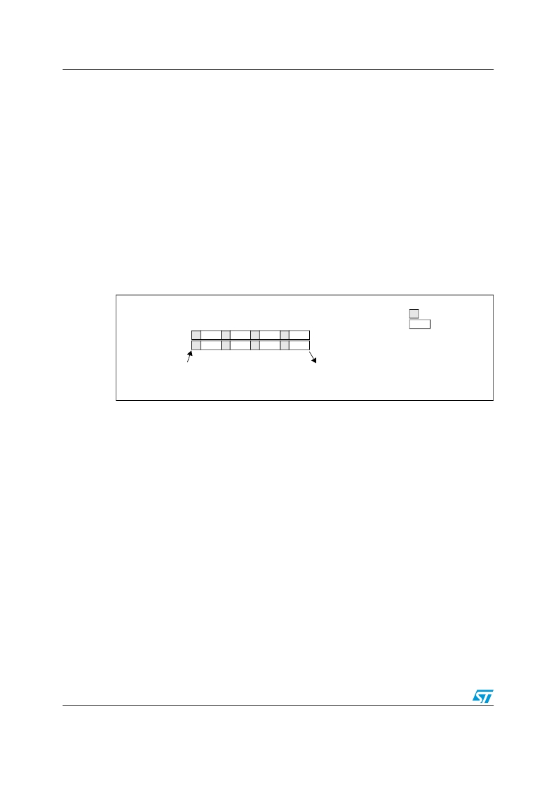
�Figure� 33.� Injected� simultaneous� mode� on� 4� channels�
�Sampling�
�Conversion�
�ADC2�
�ADC1�
�CH0�
�CH3�
�CH1�
�CH2�
�CH2�
�CH1�
�CH3�
�CH0�
�Trigger�
�End� of� injected� conversion� on� ADC1� and� ADC2�
�11.9.2�
�Note:�
�Regular� simultaneous� mode�
�This� mode� is� performed� on� a� regular� channel� group.� The� source� of� the� external� trigger�
�comes� from� the� regular� group� mux� of� ADC1� (selected� by� the� EXTSEL[2:0]� bits� in� the�
�ADC1_CR2� register).� A� simultaneous� trigger� is� provided� to� the� ADC2.�
�Do� not� convert� the� same� channel� on� the� two� ADCs� (no� overlapping� sampling� times� for� the�
�two� ADCs� when� converting� the� same� channel).�
�At� the� end� of� conversion� event� on� ADC1� or� ADC2:�
�●�
�●�
�A� 32-bit� DMA� transfer� request� is� generated� (if� DMA� bit� is� set)� which� transfers� to� SRAM�
�the� ADC1_DR� 32-bit� register� containing� the� ADC2� converted� data� in� the� upper�
�halfword� and� the� ADC1� converted� data� in� the� lower� halfword.�
�An� EOC� interrupt� is� generated� (if� enabled� on� one� of� the� two� ADC� interfaces)� when�
�ADC1/ADC2� regular� channels� are� all� converted.�
�Note:�
�212/995�
�In� regular� simultaneous� mode,� one� must� convert� sequences� with� the� same� length� or� ensure�
�that� the� interval� between� triggers� is� longer� than� the� longest� of� the� 2� sequences.� Otherwise,�
�the� ADC� with� the� shortest� sequence� may� restart� while� the� ADC� with� the� longest� sequence� is�
�completing� the� previous� conversions.�
�Doc� ID� 13902� Rev� 9�
�发布紧急采购,3分钟左右您将得到回复。
相关PDF资料
MCBTMPM330
BOARD EVAL TOSHIBA TMPM330 SER
MCIMX25WPDKJ
KIT DEVELOPMENT WINCE IMX25
MCIMX53-START-R
KIT DEVELOPMENT I.MX53
MCM69C432TQ20
IC CAM 1MB 50MHZ 100LQFP
MCP1401T-E/OT
IC MOSFET DRVR INV 500MA SOT23-5
MCP1403T-E/MF
IC MOSFET DRIVER 4.5A DUAL 8DFN
MCP1406-E/SN
IC MOSFET DVR 6A 8SOIC
MCP14628T-E/MF
IC MOSFET DVR 2A SYNC BUCK 8-DFN
相关代理商/技术参数
MCBSTM32EXLU
功能描述:开发板和工具包 - ARM EVAL BOARD + ULINK2 FOR STM32F103ZG
RoHS:否 制造商:Arduino 产品:Development Boards 工具用于评估:ATSAM3X8EA-AU 核心:ARM Cortex M3 接口类型:DAC, ICSP, JTAG, UART, USB 工作电源电压:3.3 V
MCBSTM32EXLU-ED
制造商:ARM Ltd 功能描述:KEIL STM STM32EXL EVAL BOARD
MCBSTM32EXLUME
功能描述:开发板和工具包 - ARM EVAL BOARD + ULINKME FOR STM32F103ZG
RoHS:否 制造商:Arduino 产品:Development Boards 工具用于评估:ATSAM3X8EA-AU 核心:ARM Cortex M3 接口类型:DAC, ICSP, JTAG, UART, USB 工作电源电压:3.3 V
MCBSTM32F200
功能描述:开发板和工具包 - ARM EVAL BOARD FOR STM STM32F207IG
RoHS:否 制造商:Arduino 产品:Development Boards 工具用于评估:ATSAM3X8EA-AU 核心:ARM Cortex M3 接口类型:DAC, ICSP, JTAG, UART, USB 工作电源电压:3.3 V
MCBSTM32F200U
功能描述:开发板和工具包 - ARM EVAL BOARD FOR STM STM32F207IG + ULINK2
RoHS:否 制造商:Arduino 产品:Development Boards 工具用于评估:ATSAM3X8EA-AU 核心:ARM Cortex M3 接口类型:DAC, ICSP, JTAG, UART, USB 工作电源电压:3.3 V
MCBSTM32F200UME
功能描述:开发板和工具包 - ARM EVAL BOARD FOR STM STM32F207IG ULINK-ME
RoHS:否 制造商:Arduino 产品:Development Boards 工具用于评估:ATSAM3X8EA-AU 核心:ARM Cortex M3 接口类型:DAC, ICSP, JTAG, UART, USB 工作电源电压:3.3 V
MCBSTM32F200UME-ED
制造商:ARM Ltd 功能描述:KEIL STM32F207IG EVAL BOARD
MCBSTM32F400
功能描述:开发板和工具包 - ARM EVAL BOARD FOR STM STM32F407IG
RoHS:否 制造商:Arduino 产品:Development Boards 工具用于评估:ATSAM3X8EA-AU 核心:ARM Cortex M3 接口类型:DAC, ICSP, JTAG, UART, USB 工作电源电压:3.3 V